Journals > > Topics > Integrated Optics
Integrated Optics|6 Article(s)
Research Progress in Optoelectronics Integration Technology Based on Piezoelectric Effect(Invited)
Jian SHEN, Chenglong FENG, Xun ZHANG, Lei ZHANG, Chang SHU, Yong ZHANG, and Yikai SU
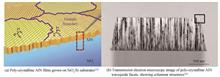
Optical communication and interconnection technology utilize photons instead of electrons as information carrier, enabling large-capacity and high-speed information transmission. Silicon-based photonics integrated circuits are expected to promote the breakthroughs for the optoelectronics chips in the“post-Moore era”due to its advantages of small size, high integration, low power consumption, and compatibility with the Complementary Metal Oxide Semiconductor (CMOS) process. So far, optoelectronic integrated chips based on silicon platforms have achieved tremendous success in industries such as coherent optical communication. However, central symmetric structures represented by silicon lack linear and high-order nonlinear effects, posing a natural disadvantage in the design and fabrication of low-power tuning devices, high-speed modulation devices, and nonlinear devices. In order to meet the low-power-consumption, high-efficiency, and large-scale integration requirements for the next generation of optoelectronic integrated chips, it is necessary to explore new effects and new thin-film materials for the development of integrated optoelectronic devices.Piezoelectric effect is an important physical phenomenon that realizes the conversion between electrical energy and mechanical energy. Some specific crystalline materials generate positive and negative charges when external mechanical force or pressure is applied, creating an electric field. When an external electric field is applied to these crystalline materials, they undergo deformation, resulting in a change in refractive index. Thanks to the progress and maturity of thin film growth and deposition techniques such as Atomic Layer Deposition (ALD) and Molecular Beam Epitaxy (MBE), many low-loss, high-piezoelectric-coefficient thin films have been prepared and realized, such as aluminum nitride (AlN), lead zirconate titanate (PZT), hafnium dioxide (HfO2), lithium niobate (LN), etc. Optical tuning based on the piezoelectric effect is a consequence of the electric field influence. Compared to thermos-optic modulation in silicon materials, piezoelectric-driven power consumption can be reduced by three to five orders of magnitude, which is of great significance for achieving low-power-consumption and large-scale optoelectronic integrated chips in applications with response frequencies ranging from KHz to GHz. Researchers have successfully developed a series of optoelectronic integrated devices through heterogeneous integration, dry etching, spin-coating polarization, and other technical approaches. These devices exhibit outstanding characteristics, including ultra-low power consumption, high efficiency, and rapid response, providing unique advantages in silicon-based optoelectronic integrated devices. Some of these materials are already compatible with CMOS processes and have shown rapid development, with promising applications demonstrating their excellent potential.An external electric field can manipulate the deformation of the thin film material by the piezoelectric effect, thereby changing the refractive index and achieving electro-optic tuning and acousto-optic modulation. This paper starts by providing an overview of the ongoing research efforts in common piezoelectric thin-film materials, including AlN, PZT, HfO2, and LN. We focus on the preparation methods and crystal orientations of the reported piezoelectric thin films. The effects of elemental doping and process conditions on the piezoelectric properties of various types of films are summarized. Subsequently, it delves into a comprehensive review and discussion of integrated photonic devices founded on piezo-optomechanical actuators, consisting of low-power-consumption piezo-optomechanically tuning devices and acousto-optic modulators. We analyze the principles of low-power-consumption piezoelectric tunable devices and summarize the performance of tunable devices (e.g., tuning efficiency, tuning power consumption, footprint, propagation loss, and response time) on different piezoelectric thin-film platforms, such as hybrid PZT-Si waveguide, PZT-SiN waveguide, AlN-SiN waveguide, and HfO2-Si waveguide. Since surface acoustic waves and light waves are confined well in the photonic integrated circuits, the coupling between the acoustic and optical fields will be significantly enhanced. We summarize the design structure, modulation efficiency, conversion efficiency, and excitation frequency of these acousto-optic modulators. Finally, the paper introduces and looks forward to the application of piezoelectric tuning devices and acousto-optic modulators, and analyzes the challenges and problems in their large-scale application. Photonic integrated chips based on the piezoelectric thin films play an important role in the applications such as optical computing, optical frequency comb generation, and LIDAR, providing a valuable solution with low power consumption. With the increasing maturity of integrated photonics technology and fabrication technology for the piezoelectric thin film, the optoelectronic integration technology based on piezoelectric effect shows good application prospects. Optical communication and interconnection technology utilize photons instead of electrons as information carrier, enabling large-capacity and high-speed information transmission. Silicon-based photonics integrated circuits are expected to promote the breakthroughs for the optoelectronics chips in the“post-Moore era”due to its advantages of small size, high integration, low power consumption, and compatibility with the Complementary Metal Oxide Semiconductor (CMOS) process. So far, optoelectronic integrated chips based on silicon platforms have achieved tremendous success in industries such as coherent optical communication. However, central symmetric structures represented by silicon lack linear and high-order nonlinear effects, posing a natural disadvantage in the design and fabrication of low-power tuning devices, high-speed modulation devices, and nonlinear devices. In order to meet the low-power-consumption, high-efficiency, and large-scale integration requirements for the next generation of optoelectronic integrated chips, it is necessary to explore new effects and new thin-film materials for the development of integrated optoelectronic devices.Piezoelectric effect is an important physical phenomenon that realizes the conversion between electrical energy and mechanical energy. Some specific crystalline materials generate positive and negative charges when external mechanical force or pressure is applied, creating an electric field. When an external electric field is applied to these crystalline materials, they undergo deformation, resulting in a change in refractive index. Thanks to the progress and maturity of thin film growth and deposition techniques such as Atomic Layer Deposition (ALD) and Molecular Beam Epitaxy (MBE), many low-loss, high-piezoelectric-coefficient thin films have been prepared and realized, such as aluminum nitride (AlN), lead zirconate titanate (PZT), hafnium dioxide (HfO2), lithium niobate (LN), etc. Optical tuning based on the piezoelectric effect is a consequence of the electric field influence. Compared to thermos-optic modulation in silicon materials, piezoelectric-driven power consumption can be reduced by three to five orders of magnitude, which is of great significance for achieving low-power-consumption and large-scale optoelectronic integrated chips in applications with response frequencies ranging from KHz to GHz. Researchers have successfully developed a series of optoelectronic integrated devices through heterogeneous integration, dry etching, spin-coating polarization, and other technical approaches. These devices exhibit outstanding characteristics, including ultra-low power consumption, high efficiency, and rapid response, providing unique advantages in silicon-based optoelectronic integrated devices. Some of these materials are already compatible with CMOS processes and have shown rapid development, with promising applications demonstrating their excellent potential.An external electric field can manipulate the deformation of the thin film material by the piezoelectric effect, thereby changing the refractive index and achieving electro-optic tuning and acousto-optic modulation. This paper starts by providing an overview of the ongoing research efforts in common piezoelectric thin-film materials, including AlN, PZT, HfO2, and LN. We focus on the preparation methods and crystal orientations of the reported piezoelectric thin films. The effects of elemental doping and process conditions on the piezoelectric properties of various types of films are summarized. Subsequently, it delves into a comprehensive review and discussion of integrated photonic devices founded on piezo-optomechanical actuators, consisting of low-power-consumption piezo-optomechanically tuning devices and acousto-optic modulators. We analyze the principles of low-power-consumption piezoelectric tunable devices and summarize the performance of tunable devices (e.g., tuning efficiency, tuning power consumption, footprint, propagation loss, and response time) on different piezoelectric thin-film platforms, such as hybrid PZT-Si waveguide, PZT-SiN waveguide, AlN-SiN waveguide, and HfO2-Si waveguide. Since surface acoustic waves and light waves are confined well in the photonic integrated circuits, the coupling between the acoustic and optical fields will be significantly enhanced. We summarize the design structure, modulation efficiency, conversion efficiency, and excitation frequency of these acousto-optic modulators. Finally, the paper introduces and looks forward to the application of piezoelectric tuning devices and acousto-optic modulators, and analyzes the challenges and problems in their large-scale application. Photonic integrated chips based on the piezoelectric thin films play an important role in the applications such as optical computing, optical frequency comb generation, and LIDAR, providing a valuable solution with low power consumption. With the increasing maturity of integrated photonics technology and fabrication technology for the piezoelectric thin film, the optoelectronic integration technology based on piezoelectric effect shows good application prospects.
Acta Photonica Sinica
- Publication Date: Nov. 25, 2023
- Vol. 52, Issue 11, 1113001 (2023)


Design of a Reconfigurable Optical Filter Based on Triple-ring-assisted Mach-Zenhnder Interferometer with Large Bandwidth Tuning Capability
Jia JIANG, Minming GENG, Qiang LIU, and Zhenrong ZHANG
A compact reconfigurable optical filter based on silicon-on-insulator with large bandwidth tuning capability is designed in this paper. The device is based on triple-ring-assisted Mach-Zehnder interferometer. The bandwidth and center wavelength of the device can be tuned at the same time by reasonably changing the phases of the microring resonators through the thermo-optic effect of silicon. The performance of the proposed device is simulated by finite difference time domain method. The simulation results show that the tuning range of the bandwidth is 1.4 nm to 10.6 nm, which accounts for 11.5% to 85% of the free spectrum range. The stopband extinction ratio is greater than 20 dB, and the passband loss is 0.4 dB to 0.7 dB, the footprint of the device is about 40 μm×60 μm. A compact reconfigurable optical filter based on silicon-on-insulator with large bandwidth tuning capability is designed in this paper. The device is based on triple-ring-assisted Mach-Zehnder interferometer. The bandwidth and center wavelength of the device can be tuned at the same time by reasonably changing the phases of the microring resonators through the thermo-optic effect of silicon. The performance of the proposed device is simulated by finite difference time domain method. The simulation results show that the tuning range of the bandwidth is 1.4 nm to 10.6 nm, which accounts for 11.5% to 85% of the free spectrum range. The stopband extinction ratio is greater than 20 dB, and the passband loss is 0.4 dB to 0.7 dB, the footprint of the device is about 40 μm×60 μm.
Acta Photonica Sinica
- Publication Date: Jul. 25, 2021
- Vol. 50, Issue 7, 275 (2021)
Precision Measurement and Theoretical Analysis of SOI Waveguide Transmission Loss and Butt-coupling Loss
Ting YU, Zhuo CHEN, Tiancheng LI, and Degui SUN
The method of Fabry-Perot resonant cavity (also called F-P cavity) is exploited to measure the optical transmission loss of SOI waveguides and the fiber-chip butt-coupling loss, with which three SOI waveguide channels having the same size and a length of 8.37 mm are measured. Then, the average value of SOI waveguide optical transmission loss/butt-coupling loss and the measurement accuracies are obtained, and the standard deviation of the measurements is very small. Another SOI waveguide with a length of 12.5 mm is measured using an automatic temperature control scanner and both the transmission losses and the butt-coupling losses of three repeated measurements are the same as one another, implying the stable measuring accuracies of F-P cavity method. The dual dependences of the measurement accuracy da/a of SOI waveguide transmission loss on the relative error dtM/tM of F-P cavity output extinction ratio and the relative error dR/R of the Fresnel reflection coefficient of SOI waveguide end-face are theoretically modelled. The simulation results show that the changes of SOI waveguide refractive index, the upper/lower cladding layers and core layer have no impacts upon the measurement accuracies of both the optical transmission loss and the fiber-chip coupling loss.The numerical simulation results are consistent with the experimental results. The method of Fabry-Perot resonant cavity (also called F-P cavity) is exploited to measure the optical transmission loss of SOI waveguides and the fiber-chip butt-coupling loss, with which three SOI waveguide channels having the same size and a length of 8.37 mm are measured. Then, the average value of SOI waveguide optical transmission loss/butt-coupling loss and the measurement accuracies are obtained, and the standard deviation of the measurements is very small. Another SOI waveguide with a length of 12.5 mm is measured using an automatic temperature control scanner and both the transmission losses and the butt-coupling losses of three repeated measurements are the same as one another, implying the stable measuring accuracies of F-P cavity method. The dual dependences of the measurement accuracy da/a of SOI waveguide transmission loss on the relative error dtM/tM of F-P cavity output extinction ratio and the relative error dR/R of the Fresnel reflection coefficient of SOI waveguide end-face are theoretically modelled. The simulation results show that the changes of SOI waveguide refractive index, the upper/lower cladding layers and core layer have no impacts upon the measurement accuracies of both the optical transmission loss and the fiber-chip coupling loss.The numerical simulation results are consistent with the experimental results.
Acta Photonica Sinica
- Publication Date: Jul. 25, 2021
- Vol. 50, Issue 7, 268 (2021)
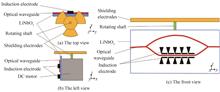
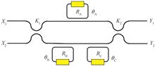
Design and Implementation of Integrated Optical Waveguide DC Electric Field Sensor
Jianxin ZHANG, Jiahong ZHANG, and Fushen CHEN
To solve the problem that the integrated optical waveguide electric field sensor can not directly respond to the DC electric field, based on the basic principle of the field milling electric field sensor, a DC electric field sensor composed of a DC motor, a shield electrode, an integrated optical waveguide Mach-Zehnder Interferometer (MZI), and an induction electrode is designed. Its volume is 87.5 mm×58.5 mm×17.5 mm. The working principle of the integrated optical waveguide DC electric field sensor is derived and a three-dimensional simulation model of the sensor is constructed using the COMSOL software. The simulation results show that the electric field intensity on the sensing electrode changes periodically with the rotation of the shielding electrode. A DC electric field experimental measurement system is established to test the dynamic range of the integrated optical waveguide DC electric field sensor. The results show that the minimum measurable electric field of the sensor is 5 kV/m, the maximum measurable electric field is greater than 140 kV/m, and the linear correlation coefficient is 0.995 1, which is suitable for DC electric field measurement. To solve the problem that the integrated optical waveguide electric field sensor can not directly respond to the DC electric field, based on the basic principle of the field milling electric field sensor, a DC electric field sensor composed of a DC motor, a shield electrode, an integrated optical waveguide Mach-Zehnder Interferometer (MZI), and an induction electrode is designed. Its volume is 87.5 mm×58.5 mm×17.5 mm. The working principle of the integrated optical waveguide DC electric field sensor is derived and a three-dimensional simulation model of the sensor is constructed using the COMSOL software. The simulation results show that the electric field intensity on the sensing electrode changes periodically with the rotation of the shielding electrode. A DC electric field experimental measurement system is established to test the dynamic range of the integrated optical waveguide DC electric field sensor. The results show that the minimum measurable electric field of the sensor is 5 kV/m, the maximum measurable electric field is greater than 140 kV/m, and the linear correlation coefficient is 0.995 1, which is suitable for DC electric field measurement.
Acta Photonica Sinica
- Publication Date: May. 25, 2021
- Vol. 50, Issue 5, 59 (2021)
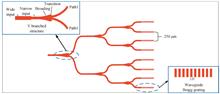
Integrated Optical Chip Based on Y-branch and Bragg Grating Structure
Xiaojie YIN, Zhiyuan ZHENG, Xingzhuang ZI, and Mingju CHAO
A 1×8 optical splitter integrated chip with channel monitoring function was fabricated by integrating Y-branch with deep etched Bragg grating structure. The integrated optical chip after coupling and packaging realizes stable optical signal transmission and monitoring function at the same time in the channel. The central wavelength range of 8-channel reflectance spectrum of the integrated optical chip is 1 597 nm~1 639 nm, with an interval of 6 nm. The maximum of 3 dB bandwidth is 0.67 nm, and the minimum of channel reflectance is 88.24%. The average insertion loss of 8 channels is 11.92 dB and the output uniformity is 0.19 dB in the wavelength of 1 550 nm. The integrated optical chip designed and fabricated in this study has simple structure and high integration, which can be widely used in the construction of fiber to home and other optical network transmission, and realize the function of real-time monitoring of network link status. A 1×8 optical splitter integrated chip with channel monitoring function was fabricated by integrating Y-branch with deep etched Bragg grating structure. The integrated optical chip after coupling and packaging realizes stable optical signal transmission and monitoring function at the same time in the channel. The central wavelength range of 8-channel reflectance spectrum of the integrated optical chip is 1 597 nm~1 639 nm, with an interval of 6 nm. The maximum of 3 dB bandwidth is 0.67 nm, and the minimum of channel reflectance is 88.24%. The average insertion loss of 8 channels is 11.92 dB and the output uniformity is 0.19 dB in the wavelength of 1 550 nm. The integrated optical chip designed and fabricated in this study has simple structure and high integration, which can be widely used in the construction of fiber to home and other optical network transmission, and realize the function of real-time monitoring of network link status.
Acta Photonica Sinica
- Publication Date: May. 25, 2021
- Vol. 50, Issue 5, 53 (2021)

Research on Designing Approaches for Device and Integration of Photonic Integrated Interferometric Detecting System
Hongjie DING, Peng LIU, Yong LIU, Hong CHANG, Shouqian CHEN, and Wang ZHANG
Based on the wave effect of light wave, the optical path matching waveguides, array waveguide gratings, phase modulators and multimode interference couplers are designed by using the beam propagation method. On this basis, the coupling characteristics of the photonic integrated device are analyzed and calculated, and a complete photonic integrated chip is designed. Through the analysis, research and optimization of each module of the photonic integrated interferometry system, an electronic prototype of the photonic integrated interferometry detection system is designed. The results show that the minimum loss of the designed photonic integrated device is 0.07 dB, and the loss of the photonic integrated chip is 7.46 dB. When the equivalent aperture is 110 mm and the system height aperture ratio is 1∶4, the electronic prototype of the photonic integrated interference detection system has the technical indexes of 0.5 ° field of view and 5 m spatial resolution at 100 km. Based on the wave effect of light wave, the optical path matching waveguides, array waveguide gratings, phase modulators and multimode interference couplers are designed by using the beam propagation method. On this basis, the coupling characteristics of the photonic integrated device are analyzed and calculated, and a complete photonic integrated chip is designed. Through the analysis, research and optimization of each module of the photonic integrated interferometry system, an electronic prototype of the photonic integrated interferometry detection system is designed. The results show that the minimum loss of the designed photonic integrated device is 0.07 dB, and the loss of the photonic integrated chip is 7.46 dB. When the equivalent aperture is 110 mm and the system height aperture ratio is 1∶4, the electronic prototype of the photonic integrated interference detection system has the technical indexes of 0.5 ° field of view and 5 m spatial resolution at 100 km.
Acta Photonica Sinica
- Publication Date: May. 25, 2021
- Vol. 50, Issue 5, 43 (2021)
Topics
© Copyright 2018-2021 | Chinese Laser Press. All Rights Reserved 沪ICP备15018463号-20